News about the project
Project updates from Fraunhofer IAF – February 2021
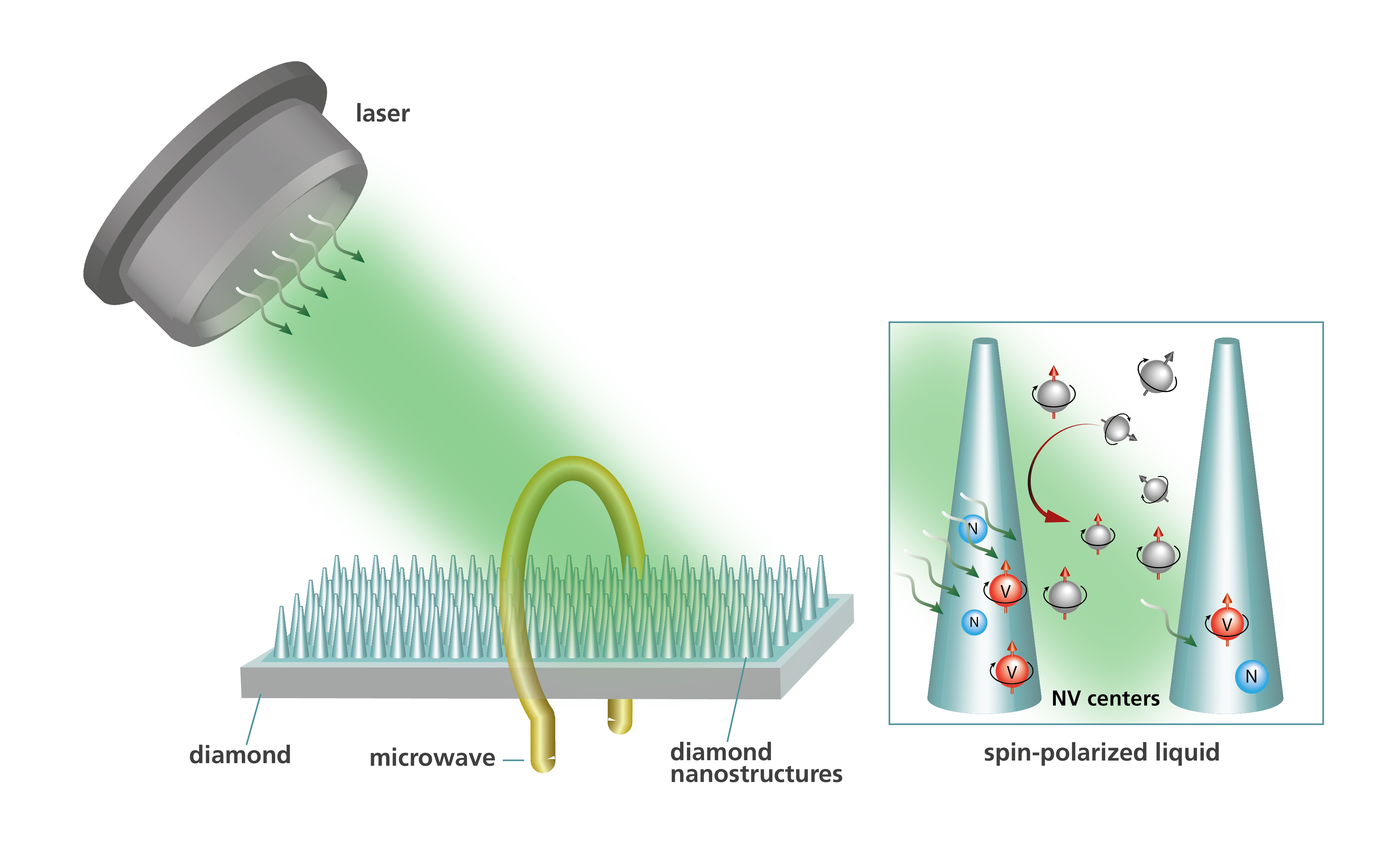
The project Metaboliqs aims to develop a novel method for hyperpolarization of metabolite molecules, which significantly improve contrast in magnetic resonance imaging. For this purpose, spin polarization will be transferred from nitrogen-vacancy (NV) color centers in diamond to the 13C atoms of the target molecules, see [1].

A successful transfer requires a close interaction of NVs with the molecules within a liquid and thus a large effective surface and NVs in the diamond close to the surface.
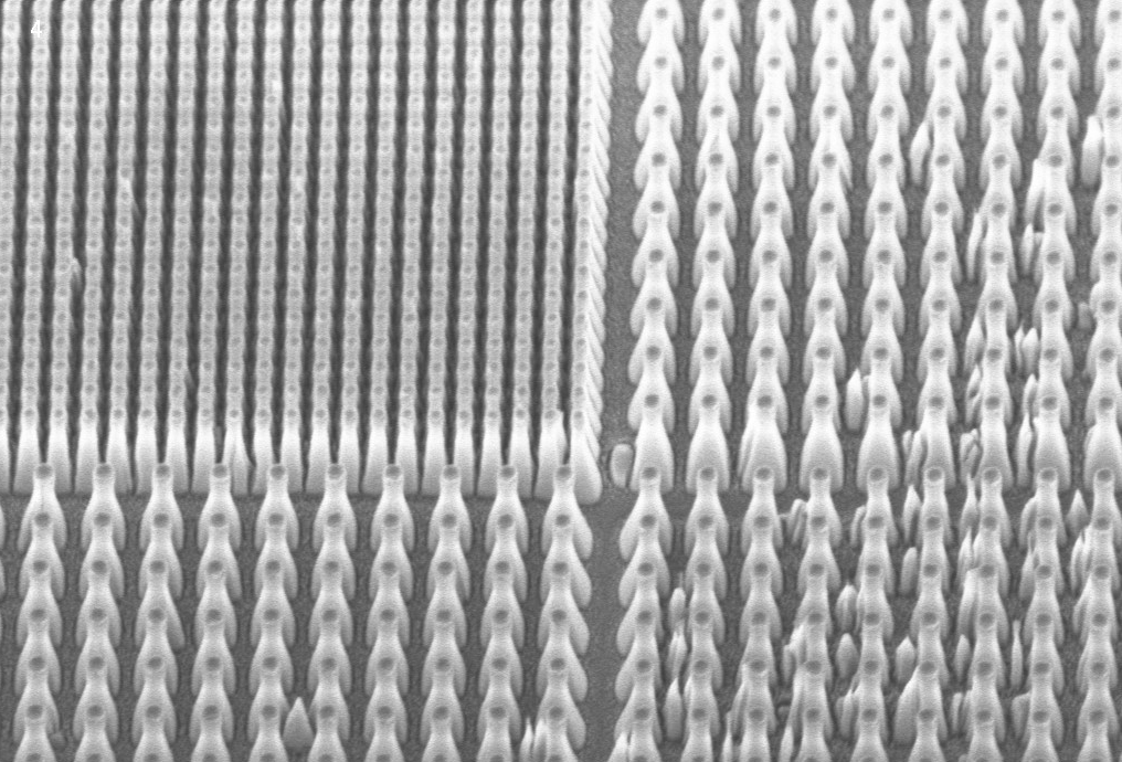
To increase the effective surface, the diamonds are patterned by e-beam lithography and three-dimensional nanostructures are created using a dry chemical etching process. The process results in arrays of nanopillars with adjustable distance and surface enhancement up to a factor of 15.
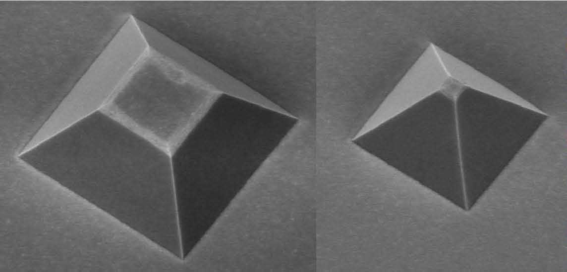
In a further step, these structures are overgrown with very thin nitrogen-doped diamond layers with a thickness of less than 100 nanometers using plasma-assisted chemical vapour deposition. To maintain the necessary high crystal quality of the diamond, first a buffer is grown to achieve well-defined {111} facets. In equilibrium, completed or truncated pyramids are formed as shown in [3].
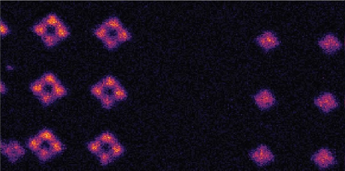
By carefully controlling the growth parameter, orientation-selective growth can be achieved. As a consequence the nitrogen-doped diamond grows only at the {111}-oriented side walls of the pyramids. Photoluminescence reveals that only those side walls shows emission from NVs.
The developed method not only ensures increased hyperpolarization in the Metaboliqs project, but also provides a powerful tool for positioning NV centers in a controlled manner, which is of enormous importance for many further quantum technological applications.


